- 您现在的位置:买卖IC网 > Sheet目录3828 > ATMEGA169PV-8MCU (Atmel)MCU AVR 16K ISP FLASH 8MHZ 64QFN
2005 Microchip Technology Inc.
Preliminary
DS41265A-page 151
PIC16F946
12.1.5
STARTING A CONVERSION
The A/D conversion is initiated by setting the
GO/DONE bit (ADCON0<1>). When the conversion is
complete, the A/D module:
Clears the GO/DONE bit
Sets the ADIF flag (PIR1<6>)
Generates an interrupt (if enabled)
If the conversion must be aborted, the GO/DONE bit
can be cleared in software. The ADRESH:ADRESL
registers will not be updated with the partially complete
A/D
conversion
sample.
Instead,
the
ADRESH:ADRESL registers will retain the value of the
previous conversion. After an aborted conversion, a
2TAD delay is required before another acquisition can
be initiated. Following the delay, an input acquisition is
automatically started on the selected channel.
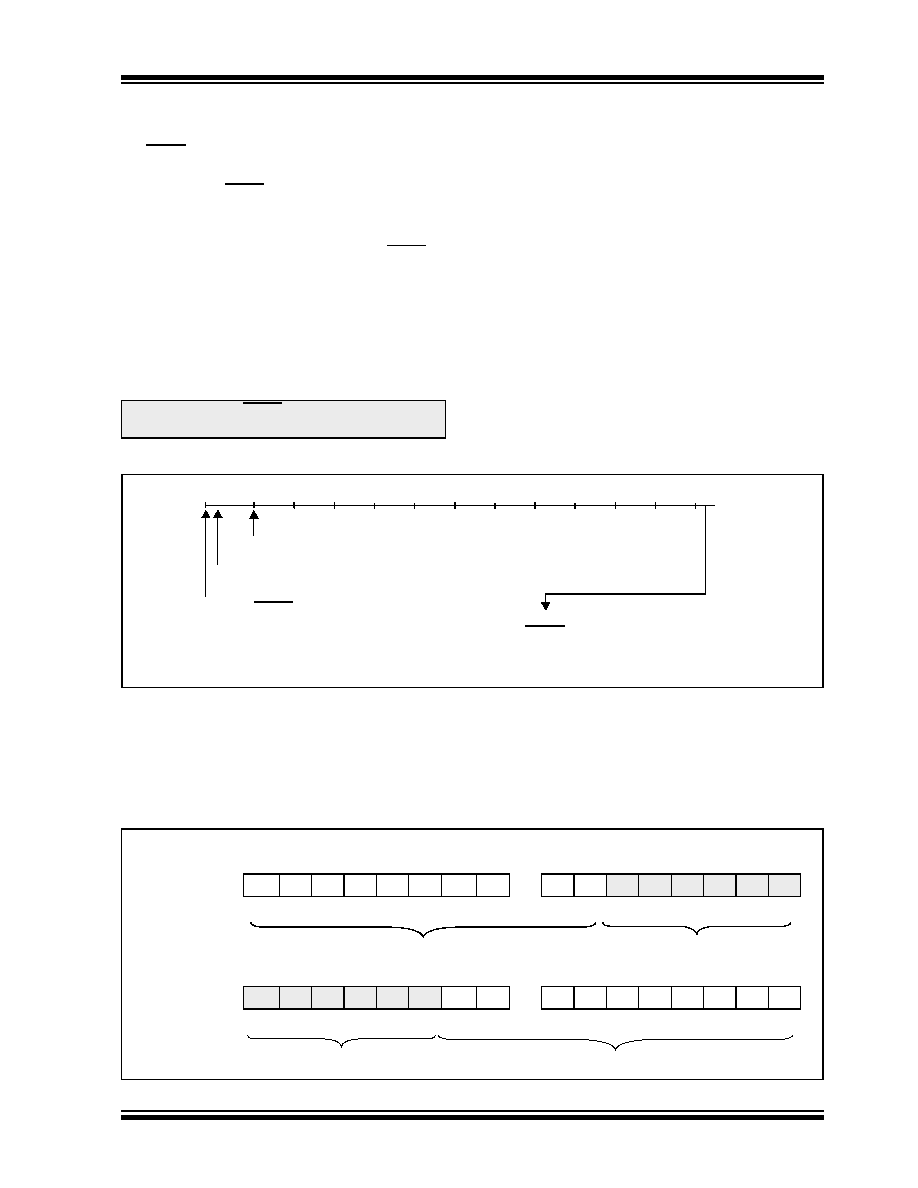
FIGURE 12-2:
A/D CONVERSION TAD CYCLES
12.1.6
CONVERSION OUTPUT
The A/D conversion can be supplied in two formats: left
or right shifted. The ADFM bit (ADCON0<7>) controls
the output format. Figure 12-3 shows the output
formats.
FIGURE 12-3:
10-BIT A/D RESULT FORMAT
Note:
The GO/DONE bit should not be set in the
same instruction that turns on the A/D.
TAD1 TAD2 TAD3 TAD4 TAD5 TAD6 TAD7 TAD8 TAD9
Set GO/DONE bit
Holding Capacitor is Disconnected from Analog Input (typically 100 ns)
b9
b8
b7
b6
b5
b4
b3
b2
TAD10 TAD11
b1
b0
TCY TO TAD
Conversion Starts
ADRESH and ADRESL registers are loaded,
GO/DONE bit is cleared,
ADIF bit is set,
Holding Capacitor is Connected to Analog Input
ADRESH
ADRESL
(ADFM = 0)MSB
LSB
bit 7
bit 0
bit 7
bit 0
10-bit A/D Result
Unimplemented: Read as ‘0’
(ADFM = 1)
MSB
LSB
bit 7
bit 0
bit 7
bit 0
Unimplemented: Read as ‘0’
10-bit A/D Result
发布紧急采购,3分钟左右您将得到回复。
相关PDF资料
ATMEGA169P-16MCU
MCU AVR 16K ISP FLSH 16MHZ 64QFN
AT91SAM7XC256-CU
MCU ARM 256K HS FLASH 100-TFBGA
PIC16LF874A-I/P
IC MCU FLASH 4KX14 EE A/D 40DIP
PIC16F84-10/SO
IC MCU FLASH 1KX14 EE 18SOIC
AT91SAM7XC128-CU
MCU ARM 128K HS FLASH 100-TFBGA
PIC18F2458-I/SO
IC PIC MCU FLASH 12KX16 28SOIC
PIC18F4455-I/P
IC PIC MCU FLASH 12KX16 40DIP
AT91SAM7X256-CU
MCU ARM 256K HS FLASH 100-TFBGA
相关代理商/技术参数
ATMEGA169PV-8MU
功能描述:8位微控制器 -MCU AVR 16K FLASH 512B EE 1K SRAM 5V RoHS:否 制造商:Silicon Labs 核心:8051 处理器系列:C8051F39x 数据总线宽度:8 bit 最大时钟频率:50 MHz 程序存储器大小:16 KB 数据 RAM 大小:1 KB 片上 ADC:Yes 工作电源电压:1.8 V to 3.6 V 工作温度范围:- 40 C to + 105 C 封装 / 箱体:QFN-20 安装风格:SMD/SMT
ATMEGA169PV-8MU SL383
制造商:Atmel Corporation 功能描述:MCU 8BIT ATMEGA RISC 16KB FLASH 2.5V/3.3V/5V 64PIN MLF - Tape and Reel
ATMEGA169PV-8MU
制造商:Atmel Corporation 功能描述:IC 8BIT MCU AVR MEGA 8MHZ 64-QFN
ATMEGA169PV-8MUR
功能描述:8位微控制器 -MCU AVR LCD 16KB FLSH EE 512B 1KB SRAM-8MHZ RoHS:否 制造商:Silicon Labs 核心:8051 处理器系列:C8051F39x 数据总线宽度:8 bit 最大时钟频率:50 MHz 程序存储器大小:16 KB 数据 RAM 大小:1 KB 片上 ADC:Yes 工作电源电压:1.8 V to 3.6 V 工作温度范围:- 40 C to + 105 C 封装 / 箱体:QFN-20 安装风格:SMD/SMT
ATMEGA169V
制造商:ATMEL 制造商全称:ATMEL Corporation 功能描述:8-bit Microcontroller with 16K Bytes In-System Programmable Flash
ATMEGA169V_06
制造商:ATMEL 制造商全称:ATMEL Corporation 功能描述:8-bit Microcontroller with 16K Bytes In-System Programmable Flash
ATMEGA169V-1AC
功能描述:IC MCU 8BIT 16KB FLASH 64TQFP 制造商:microchip technology 系列:AVR? ATmega 包装:托盘 零件状态:停產 核心处理器:AVR 核心尺寸:8-位 速度:1MHz 连接性:SPI,UART/USART,USI 外设:欠压检测/复位,LCD,POR,PWM,WDT I/O 数:53 程序存储容量:16KB(8K x 16) 程序存储器类型:闪存 EEPROM 容量:512 x 8 RAM 容量:1K x 8 电压 - 电源(Vcc/Vdd):1.8 V ~ 5.5 V 数据转换器:A/D 8x10b 振荡器类型:内部 工作温度:0°C ~ 70°C 封装/外壳:64-TQFP 供应商器件封装:64-TQFP(14x14) 基本零件编号:ATmega169 标准包装:160
ATMEGA169V-1AI
制造商:ATMEL 制造商全称:ATMEL Corporation 功能描述:8-bit AVR Microcontroller with 16K Bytes In-System Programmable Flash